New technique for measuring nanostructures
Bringing two electrical insulators together to create an electrical superconductor: Anyone wishing to analyze such phenomena in nanostructures will soon come up against metrological limitations – unless a new method is used that Würzburg physicists have helped to develop.

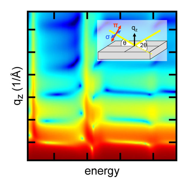
X-ray interference pattern measured while studying complex nano-layer structures. The sketch inserted illustrates the path of the x-ray beam relative to the surface of the sample.
Sebastian Macke
Modern electronic devices contain components such as transistors and diodes consisting of semiconductor layers made of silicon, germanium or gallium, and arsenic. Semiconductors made from these chemical elements have relatively simple properties that have been well characterized scientifically.
Likewise, the possible applications for such layer structures in memory modules and microprocessors are also simple: “The primary objectives of technological improvements are further miniaturization, increasing component density, and greater speed,” says physics professor Vladimir Hinkov from the University of Würzburg.
Elements that reveal interesting phenomena
On the other hand, science expects to unearth entirely new possibilities with components that contain manganese, nickel, titanium, and other elements from the so-called subgroups. “These metals have electron clouds that enable more complex bonds and electron configurations. This leads to physical phenomena that are unknown in semiconductors,” says Hinkov. As examples of such phenomena he mentions tremendous magnetoresistance and various magnetic orders, all of which occur in oxides of these metals.
Even more interesting application possibilities are opened up when these oxides are placed on top of each other in ultra-thin layers, some only a few atoms thick. For example, electrical resistance completely disappears at the interface between strontium titanate (SrTiO3) and lanthanum aluminate (LaAlO3) – despite the fact that both materials in themselves have very high electrical resistance they become a superconductor at their shared interface. So, it is no wonder that such nanostructures are the subject of intensive research.
Why the analysis of nanostructures is complicated
Chemical composition, magnetic order, distribution of electrons in the electron clouds: “Recording these properties sounds like an easy task, but in reality it is extremely complicated and conventional measurement methods can be used in very few cases,” says the Würzburg professor of physics. One reason for this is that the phenomena of interest occur in the nanocosmos, on length scales of just a few nanometers.
Of course, there are measurement methods with nanometer resolution, but these have disadvantages. One example is popular Scanning Transmission Electron Microscopy (STEM). Here, thin slices are removed from a nanostructure and scanned with an electron beam. The sample therefore has to be destroyed for the test – but doing so may change the properties that you actually want to analyze.
What the newly developed measurement method can do
With Vladimir Hinkov as the coordinator, a team of scientists from Germany, Canada, and the USA has now developed a promising new measurement method and presented it in the journal “Advanced Materials”. It works without destroying anything, offers a nanometer resolution, identifies the chemical elements involved, and is able to determine both the magnetic order and the electron distribution. Tiny traces of elements hidden deep in the nanostructure can also be identified using this method. Chemical profiles can be determined even in structures made from many elements and with complex layering.
The method, an enhancement of resonant x-ray reflectometry, is based on the scattering of x-rays with a wavelength of a few nanometers at the interfaces of the layer structure: The various scattered partial beams are then superimposed and measured. The measurements are processed accordingly to deliver an image of the structure with depth resolution. In this approach, the method resembles optical holography, which is used to generate images with spatial resolution.
Why success was dependent on many specialists
“An undertaking of this magnitude was only possible with the involvement of colleagues from many different disciplines,” says Hinkov. First you need x-ray light of such high intensity and quality as can only be generated using synchrotrons. The measurements are taken using highly specialized instruments, which the researchers set up on the synchrotron itself.
In addition, nanostructures of the highest quality are required in order to refine and test the method. The measurement data are analyzed using specially developed software and, finally, the results need to be discussed with theoreticians to arrive at a better understanding of the phenomena.
The next steps in the research
“We have been working intensively on this project for several years, and now our patience has really paid off,” says the Würzburg physicist happily. While it is true that the layer structures examined are not yet components for applications, the materials used are technologically relevant and the next development stages are clear: “Research into structures with interesting magnetic and electronic properties and, in the not too distant future, the design of elements with customized physical and technological properties,” explains Hinkov. Switchable magnetism, superconductivity, and novel sensors are some of the applications that offer promising possibilities here.


