High-resolution measurement of photocurrents
The continuing trend toward miniaturization in electronics demands the use of new materials. Components made of carbon nanotubes may meet this need – and the properties of single nanotube devices can now be characterized with the required resolution.
Given the demand for further miniaturization of electronic components, current silicon-based technology will soon reach its limits, set by fundamental physical and technical parameters. Minute hollow cylinders made from sheets of carbon, so-called carbon nanotubes, have the potential to exceed these limits. Not only can single carbon nanotubes be utilized as transistors, they can also absorb and emit light.
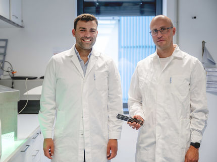
The walls of these tubes are around 1 nanometer (nm) thick. Ideally, their optical and electrical properties should be characterized at a comparable scale. LMU professorAchim Hartschuhand his team have used an optical antenna – a tiny gold pin with a sharp tip that is irradiated with a laser – to simultaneously measure electrical and optical signals from nanotubes with nanoscale precision. Conventional methods based on confocal microscopy do not attain this level of spatial resolution.
Characterizing devices made of nanotubes
Using an optical antenna allows one to amplify the signals emitted by single nanotubes and map these with very high resolution. “In our study, we have measured photocurrents along single carbon nanotubes with a resolution of less than 30 nm,” says Hartschuh. He and his colleagues have already used this method, called tip-amplified optical near-field microscopy, in many other settings, and have now developed it still further.
The spatial resolution of the photocurrent measurements corresponds closely to the theoretically expected level. And Hartschuh, who is a member of LMU’s Center for NanoScience (CeNS) and is involved in the Nanosystems Initiative Munich (NIM) points to further possible applications of the technique: “In addition to the carbon nanotubes employed here, our method could be applied to inorganic semiconducting nanowires, and perhaps to solar cells and the materials used to fabricate them,” he says.
Original publication
Other news from the department science

Get the analytics and lab tech industry in your inbox
By submitting this form you agree that LUMITOS AG will send you the newsletter(s) selected above by email. Your data will not be passed on to third parties. Your data will be stored and processed in accordance with our data protection regulations. LUMITOS may contact you by email for the purpose of advertising or market and opinion surveys. You can revoke your consent at any time without giving reasons to LUMITOS AG, Ernst-Augustin-Str. 2, 12489 Berlin, Germany or by e-mail at revoke@lumitos.com with effect for the future. In addition, each email contains a link to unsubscribe from the corresponding newsletter.


