Nanotechnologists gain powerful new materials probe
Researchers at the National Institute of Standards and Technology (NIST) and The Johns Hopkins University have constructed a unique tool for exploring the properties of promising new materials with unprecedented sensitivity and speed — potentially allowing them to identify quickly those most useful for nanotechnology and industrial applications.
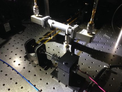
This novel instrument, called the Multi-Axis Crystal Spectrometer (MACS), is a variation on several other spectrometers at the NIST Center for Neutron Research (NCNR), where MACS is located. Like them, MACS bombards a sample of material with low-energy neutrons, which then bounce off the sample’s constituent atoms in specific directions and with specific velocities that reflect the arrangement of atoms within the material. Analyzing how neutrons scatter from a sample can tell scientists a great deal about the material’s physical properties, but older spectrometers are limited to relatively large samples and offer less range in the conditions under which they can be tested.
“These limitations are problematic in nanotechnology,” says Professor Collin Broholm of the Johns Hopkins University, “because oftentimes you grow a new material as a tiny crystal weighing only four or five milligrams, and then you want to see how it behaves under, say, an intense magnetic field.”
Not only can MACS overcome these limitations, but its unique construction allow has additional advantages. Many spectrometers provide just a single “channel” for detection, whereas MACS offers 20, forming a semicircle behind the sample — an arrangement that leads Broholm to compare MACS to a wide-angle, high-resolution lens. These improvements mean that MACS could become a favorite tool for scientists who must choose — and choose quickly — what material to grow next.
“With previous instruments for inelastic scattering from magnetic materials, 80 milligrams is about the smallest sample you can work with,” Broholm says. “But with MACS, we might be able to get detailed information about magnetic interactions even from a nano-structured thin film sample. These are the sort of interactions that nanotechnologists are trying to take advantage of when they design and shape things at the nanoscale.”
Most read news
Organizations
Other news from the department research and development
These products might interest you

Get the analytics and lab tech industry in your inbox
By submitting this form you agree that LUMITOS AG will send you the newsletter(s) selected above by email. Your data will not be passed on to third parties. Your data will be stored and processed in accordance with our data protection regulations. LUMITOS may contact you by email for the purpose of advertising or market and opinion surveys. You can revoke your consent at any time without giving reasons to LUMITOS AG, Ernst-Augustin-Str. 2, 12489 Berlin, Germany or by e-mail at revoke@lumitos.com with effect for the future. In addition, each email contains a link to unsubscribe from the corresponding newsletter.
