Detecting light in a different dimension
Polymer nanostructures longer than wide make graphene a better light detector
Scientists from the Center for Functional nanomaterials (CFN) have dramatically improved the response of graphene to light through self-assembling wire-like nanostructures that conduct electricity. The improvement could pave the way for the development of graphene-based detectors that can quickly sense light at very low levels, such as those found in medical imaging, radiation detection, and surveillance applications.
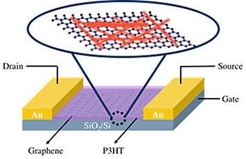
Cartoon of the graphene-P3HT nanowire hybrid field-effect transistor. Placing the nanowire mesh (red) on top of the graphene (purple) improves the device's response to light. The silicon dioxide/silicon (grey) substrate, or "gate" electrode, controls the flow of electrical current between the electron source and drain (in this case, Au, or gold, electrodes). The scientists used electron-beam lithography to pattern the device.
ACS Photonics, Oct. 12, 2018
Graphene is a two-dimensional (2-D) nanomaterial with unusual and useful mechanical, optical, and electronic properties. It is both extremely thin and incredibly strong, detects light of almost any color, and conducts heat and electricity well. However, because graphene is made of sheets of carbon only one atom thick, it can only absorb a very small amount of incoming light (about two percent).
One approach to overcoming this problem is to combine graphene with strong light-absorbing materials, such as organic compounds that conduct electricity. Scientists recently demonstrated an improved photoresponse by placing thin films (a few tens of nanometers) of one such conductive polymer, poly(3-hexylthiophene), or P3HT, on top of a single layer of graphene.
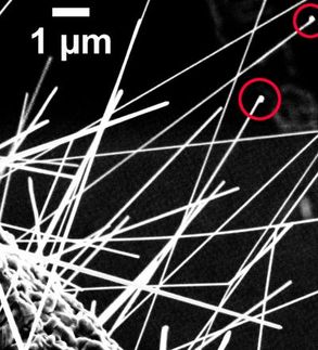
Now, the CFN scientists have improved the photoresponse by an additional 600 percent by changing the morphology (structure) of the polymer. Instead of thin films, they used a mesh of nanowires--nanostructures that are many times longer than they are wide--made of the same polymer and similar thickness
"We used self-assembly, a very simple and reproducible method, to create the nanowire mesh," said first author Mingxing Li, a research associate in the CFN Soft and Bio Nanomaterials Group. "Placed in an appropriate solution and stirred overnight, the polymer will form into wire-like nanostructures on its own. We then spin-casted the resulting nanowires onto electrical devices called graphene field-effect transistors (FETs)."
The scientists fabricated FETs made of graphene only, graphene and P3HT thin films, and graphene and P3HT nanowires. After checking the thickness and crystal structure of the FET devices through atomic force microscopy, Raman spectroscopy, and x-ray scattering techniques, they measured their light-induced electrical properties (photoresponsivity). Their measurements of the electric current flowing through the FETs under various light illumination powers revealed that the nanowire FETs improve photoresponse by 600 percent compared to the thin film FETs and 3000 percent compared to graphene-only FETs.
"We did not expect to see such a dramatic improvement just by changing the morphology of the polymer," said co-corresponding author Mircea Cotlet, a materials scientist in the CFN Soft and Bio Nanomaterials Group.
The scientists believe that there are two explanations behind their observations.
"At a certain polymer concentration, the nanowires have dimensions comparable to the wavelength of light," said Li. "This size similarity has the effect of increasing light scattering and absorption. In addition, crystallization of P3HT molecules within the nanowires provides more charge carriers to transfer electricity to the graphene layer."
"In contrast to conventional thin films where polymer chains and crystals are mostly randomly oriented, the nanoscale dimension of the wires forces the polymer chains and crystals into a specific orientation, enhancing both light absorption and charge transfer," said co-author Dmytro Nykyphanchuck, a materials scientist in the CFN Soft and Bio Nanomaterials Group.
The scientists have filed a U.S. patent for their fabrication process, and they are excited to explore light-matter interactions in other 2-D--as well as 0-D and 1-D--materials.
"Plasmonics and nanophotonics--the study of light at the nanometer scale--are emerging research areas," said Cotlet, who earlier this year co-organized a workshop for user communities of the CFN and the National Synchrotron Light Source II (NSLS-II)--another DOE Office of Science User Facility at Brookhaven--to explore frontiers in these areas. "Nanostructures can manipulate and control light at the nanoscale in very interesting ways. The advanced nanofabrication and nanocharacterization tools at the CFN and NSLS-II are perfectly suited for creating and studying materials with enhanced optoeletronic properties."
Original publication
Other news from the department science