Filming light and electrons coupled together as they travel under cover
In a breakthrough for future optical-electronic hybrid computers, scientists at EPFL have developed an ultrafast technique that can track light and electrons as they travel through a nanostructured surface.

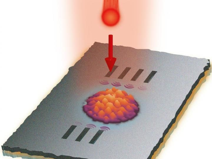
An illustration of the experimental set-up described in this study
F. Carbone/EPFL
When light couples to electrons on a surface, their concerted motion can travel as a wave guided by the surface geometry itself. These waves are known as "surface plasmons" and might be useful in telecommunications and future computing, where data will be shuttled across processors using light instead of electricity. Aside from being more energy-efficient, these processors could be miniaturized down to the nanoscale to build high-resolution sensors and nanosized signal processing systems. But these processors would be built from stacking different layers of advanced materials and, so far, we don't have a reliable way of tracking the guided light as it moves across their interfaces. EPFL scientists have now done exactly that using a new, ultrafast method.
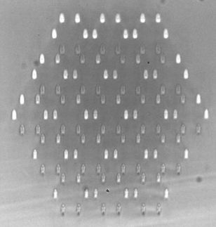
The lab of Fabrizio Carbone at EPFL led the project to create a tiny antenna array that would allow plasmons to travel across an interface. The array consisted of an extremely thin membrane of silicon nitride (50 nm thick) covered with an even thinner film of silver (30 nm thick). The scientists then "punched" a series of nano-holes through the surface that would act as the antennas -- the plasmon "hotspots".
The researchers then fired ultrafast laser pulses (light) onto the array to light up the antennas. With a controlled temporal delay, ultrashort electron pulses were then fired across the multilayer stack, to map the plasmons radiated by the antennas at the interface between the silver film and the silicon nitride membrane. Using an ultrafast technique called PINEM, which can "see" surface plasmons, even when they are bound to a buried interface, the scientists were able to actually film the propagation of the guided light and read its spatial profile across the film.
"Trying to see plasmons in these interfaces between layers is a bit like trying to film people in a house from the outside," explains Fabrizio Carbone. "A regular camera won't show you anything; but if you use microwave or a similar energy-tracking imaging, you can see right through the walls."
The current paper paves the way for designing and controlling confined plasmonic fields in multilayered structures, which is key for future optoelectronic devices.
Original publication
Most read news
Original publication
Tom T. A. Lummen, Raymond J. Lamb, Gabriele Berruto, Thomas LaGrange, Luca Dal Negro, F. Javier García de Abajo, Damien McGrouther, B. Barwick & F. Carbone; "Imaging and controlling plasmonic interference fields at buried interfaces"; Nature Comm.; 2016
Topics
Organizations
Other news from the department science

Get the analytics and lab tech industry in your inbox
By submitting this form you agree that LUMITOS AG will send you the newsletter(s) selected above by email. Your data will not be passed on to third parties. Your data will be stored and processed in accordance with our data protection regulations. LUMITOS may contact you by email for the purpose of advertising or market and opinion surveys. You can revoke your consent at any time without giving reasons to LUMITOS AG, Ernst-Augustin-Str. 2, 12489 Berlin, Germany or by e-mail at revoke@lumitos.com with effect for the future. In addition, each email contains a link to unsubscribe from the corresponding newsletter.


