New electron microscopy method sculpts 3-D structures at atomic level
Electron microscopy researchers at the Department of Energy’s Oak Ridge National Laboratory have developed a unique way to build 3-D structures with finely controlled shapes as small as one to two billionths of a meter.
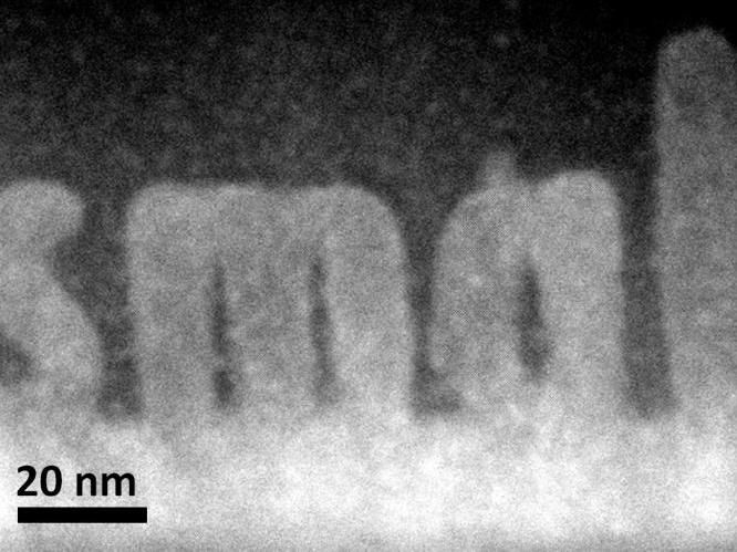
ORNL researchers used a new scanning transmission electron microscopy technique to sculpt 3-D nanoscale features in a complex oxide material.
ORNL
The ORNL study demonstrates how scanning transmission electron microscopes, normally used as imaging tools, are also capable of precision sculpting of nanometer-sized 3-D features in complex oxide materials.
By offering single atomic plane precision, the technique could find uses in fabricating structures for functional nanoscale devices such as microchips. The structures grow epitaxially, or in perfect crystalline alignment, which ensures that the same electrical and mechanical properties extend throughout the whole material.
“We can make smaller things with more precise shapes,” said ORNL’s Albina Borisevich, who led the study. “The process is also epitaxial, which gives us much more pronounced control over properties than we could accomplish with other approaches.”
ORNL scientists happened upon the method as they were imaging an imperfectly prepared strontium titanate thin film. The sample, consisting of a crystalline substrate covered by an amorphous layer of the same material, transformed as the electron beam passed through it. A team from ORNL’s Institute for Functional Imaging of Materials, which unites scientists from different disciplines, worked together to understand and exploit the discovery.
“When we exposed the amorphous layer to an electron beam, we seemed to nudge it toward adopting its preferred crystalline state,” Borisevich said. “It does that exactly where the electron beam is.” The use of a scanning transmission electron microscope, which passes an electron beam through a bulk material, sets the approach apart from lithography techniques that only pattern or manipulate a material’s surface.
“We’re using fine control of the beam to build something inside the solid itself,” said ORNL’s Stephen Jesse. “We’re making transformations that are buried deep within the structure. It would be like tunneling inside a mountain to build a house.”
The technique offers a shortcut to researchers interested in studying how materials’ characteristics change with thickness. Instead of imaging multiple samples of varying widths, scientists could use the microscopy method to add layers to the sample and simultaneously observe what happens.
“The whole premise of nanoscience is that sometimes when you shrink a material it exhibits properties that are very different than the bulk material,” Borisevich said. “Here we can control that. If we know there is a certain dependence on size, we can determine exactly where we want to be on that curve and go there.”
Theoretical calculations on ORNL’s Titan supercomputer helped the researchers understand the process’s underlying mechanisms. The simulations showed that the observed behavior, known as a knock-on process, is consistent with the electron beam transferring energy to individual atoms in the material rather than heating an area of the material.
“With the electron beam, we are injecting energy into the system and nudging where it would otherwise go by itself, given enough time,” Borisevich said. “Thermodynamically it wants to be crystalline, but this process takes a long time at room temperature.”
Original publication
Jesse, S., He, Q., Lupini, A. R., Leonard, D. N., Oxley, M. P., Ovchinnikov, O., Unocic, R. R., Tselev, A., Fuentes-Cabrera, M., Sumpter, B. G., Pennycook, S. J., Kalinin, S. V. and Borisevich, A. Y.; "Atomic-Level Sculpting of Crystalline Oxides: Toward Bulk Nanofabrication with Single Atomic Plane Precision"; Small; 2015
Other news from the department science