A bendable touch panel with silver nano ink printing
JST has recognized the results of NexTEP's project, "A Sensor Film for Touch Panels Using Thin Metallic Wire" as a success.
This development task was based on the research of Professor Tatsuo Hasegawa, Principal Research Manager at the flexible electronics Research Center of the National Institute of Advanced Industrial Science and Technology, and was consigned to Tanaka Kikinzoku Kogyo from April 2014 through September 2017. The research proceeded with the aim of practical application through Tanaka Kikinzoku Kogyo's Global Marketing/R&D Division.
In conventional electrostatic capacity-type touch panels, indium tin oxide (ITO) is used for the sensor. However, because of its high electrical resistivity and weakness upon bending, companies faced difficulties in increasing the size of such sensors and making them more flexible. Metal mesh (MM) solves these problems, but it is difficult to make thinner than 4 um, and no technology existed to manufacture the mesh via printing.
To apply the new technology (SuPR-NaP method), which fabricates wiring through an adsorption reaction between special silver ink and an activated fluororesin surface, at a suitable speed for commercial manufacturing, the project clarified the reaction mechanism and researched the development of manufacturing equipment as well as the conditions for each process. As a result, the project constructed a system for manufacturing MM film (line width: 2-4 um) with the full process roll-to-roll method. In a 200,000-frequency (radius: 2 mm) bending test, this MM film exhibits hardly any changes in resistance values, and it has cleared general reliability testing.
This success in manufacturing the world's first micro-wiring film with a full process roll-to-roll method is an important technological innovation in printed electronics for the flexible electronic device market. It is also anticipated that the technology could be applied and used for applications requiring metal patterns on resin film (function films e.g. antibacterial, catalyst, thermal insulating).
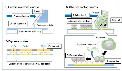
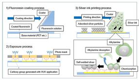
New technology (SuPR-NaP method) manufacturing processes and printing reaction mechanism: 1) Fluororesin application: Fluororesin that can repel silver ink is used to coat the base (PET film). 2) Exposure: When VUV*7 light is applied to the fluororesin surface, a carboxy group is formed. This property is used to form a carboxy group on the film in accordance with the photo mask pattern. 3) Silver nanoparticle printing: When the film is coated with silver ink after exposure, the silver nanoparticles undergo chemisorption onto the carboxy group alone. Excessive silver ink is removed by the coater (equipment used to spread out the applied liquid with a blade and scrape off excess liquid). Alkylamine, which had inhibited the aggregation of silver nanoparticles in the silver ink, is completely removed from the silver surface by postprocessing so that silver nanoparticles can fuse to each other. This makes it possible to form silver wiring with regular thickness.
Tanaka
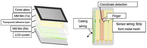
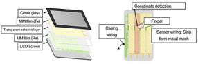
Metal mesh electrostatic capacity touch panel structure: When a finger approaches the touch panel, electrostatic capacity created between vertical and horizontal sensor wiring and the finger is detected and the finger position coordinate is identified. Simultaneous detection of multiple points is also possible. With this technology, metal mesh is used in the sensor wiring. Normally, ITO is used.
Tanaka

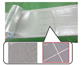
Sensor film continuously manufactured with the roll-to-roll method (7-inch pattern)
Tanaka
Context
With the increased use of information technology in society, people are demanding access to information in various locations, at various times and in various situations. Touch panels that are integrated with the display are used in many devices, from smartphones, notebooks, large panel to automotive displays.
Moreover, touch sensors now need to be compatible with not only flat panel displays, but also recently-announced three-dimensional curved and bendable displays. Transparent (conducting) electrodes using ITO are mainly used for current touch sensors. However, physical problems such as high electrical resistivity and weakness upon bending imposed limitations on responding to needs for flexibility and increasingly large screen sizes. Metal mesh(MM), in which thin metallic wire is used as the electrode, is being applied on as a material that could solve these problems. However, as the line width and pitch of current MM is thick, the wiring is visible on smartphones, which are used at a short distance. Therefore, it has only come into popular use for large displays.
Development Details
With this new printing technology, a film to which liquid-repelling fluororesin is applied undergoes pattern exposure through a photo mask. Metal ink is then scanned onto it to form the wiring. This technology means that metal wiring with a fixed film thickness can be formed by means of the chemisorption of metal nanoparticles on the fluororesin surface activated by light.
The following technology has been developed to make it possible to manufacture MM film with micro wiring that can also be used for smartphones at a low cost. The project constructed a roll-to-roll production system that has not been available with existing manufacturing methods.
- The reaction mechanism for printing was elucidated, ink and fluororesin which was investigated and a method of even printing on large areas was developed. This made it possible to fabricate a 7- to 8-inch sensor film with micro wiring (line width: 2-4 um).
- Invisible wiring was developed by postprocessing the sensor pattern design (line width and shape) to respond to market needs. As a result, a MM film that could also be used for smartphones was able to be developed. The ability of this film to withstand 200,000-frequency (radius: 2 mm) bending test was also confirmed.
- Equipment for each process was developed and a manufacturing method with the roll-to-roll process was established. In a manufacturing experiment for the line width 4 um MM film, the 10m roll length achieved more than a 95% yield rate was achieved.
Anticipated Effects
This successful development is expected to enable the low-cost manufacturing of high-functioning touch panel sensor films that can be used for three-dimensional curved or bendable displays.
This manufacturing of a micro wiring film with full process roll-to-roll process is the first of its kind in the world. It is a breakthrough technological innovation for printed electronics used in the flexible electronic device market. It is anticipated that this technology can be not only applied and used in electronics fields such as OLED displays, IoT device wiring and electrodes, but also in the manufacturing of functional films such as antibacterial films, films for catalysts and thermal insulation films.
Other news from the department science