A fast, non-destructive test for 2-dimensional materials
Thinning a material down to a single-atom thickness can dramatically change that material's physical properties. For example, graphene, the best-known 2D material, has unparalleled strength and electrical conductivity, unlike its bulk form, graphite. Researchers have begun to study hundreds of other 2D materials for the purposes of electronics, sensing, early cancer diagnosis, water desalination and a host of other applications. Now, a team of Penn State researchers in the Department of Physics and the Center for Two-Dimensional and layered materials (2DLM) has developed a fast, nondestructive optical method for analyzing defects in 2D materials.
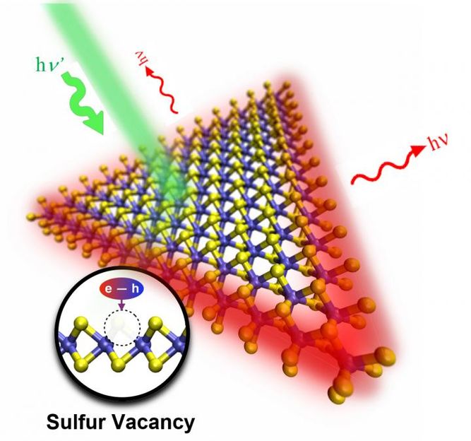
Molecular model of a WS2 triangular monolayer targeted with a green laser (hv'). Red light (hv) is emitted from the edges where defects consisting of sulfur vacancies are located. Electron-hole pairs are bound at the vacancy site (see inset).
Yuanxi Wang, Penn State
"In the semiconductor industry, for example, defects are important because you can control properties through defects," said Mauricio Terrones, professor of physics, materials science and engineering and chemistry. "This is known as defect engineering. Industry knows how to control defects and which types are good for devices."
To really understand what is going on in a 2D material like tungsten disulfide, which has a single atom-thick layer of tungsten sandwiched between two atomic layers of sulfur, would require a high-power electron microscope capable of seeing individual atoms and the holes, called vacancies, where the atoms are missing.

"The benefit of transmission electron microscopy (TEM) is that you get an image and you can see directly what is going on -- you get direct evidence," said Bernd Kabius, staff scientist at Penn State's Materials Research Institute, an expert in TEM and a coauthor on the paper
The downsides, according to Kabius, are an increased possibility of damage to the delicate 2D material, the complex preparation required of the sample, and the time involved -- an entire day of instrument time to image a single sample and a week or more to interpret the results. For those reasons, and others, researchers would like to combine TEM with another method of looking at the sample that is simpler and faster.
The technique developed by Terrones and his team uses an optical method, fluorescent microscopy, in which a laser of a specific wavelength is shone on a sample. The excited electrons, pushed to a higher energy level, each emit a photon of a longer wavelength when they drop down to a lower energy level. The longer wavelength can be measured by spectroscopy and gives information about the defect type and location on the sample. The team can then correlate the results with visual confirmation under the TEM. Theoretical calculations also helped to validate the optical results.
The sample must be placed in a temperature-controlled specimen holder and the temperature lowered to 77 Kelvin, almost 200 degrees Celsius below zero. At this temperature, the electron-hole pairs that produce the fluorescence are bound to the defect -- in the case of this work a group of sulfur vacancies in the top layer of the sandwich -- and emit a signal stronger than the pristine areas of the material.
"For the first time, we have established a direct relationship between the optical response and the amount of atomic defects in two-dimensional materials," said Victor Carozo, former postdoctoral scholar in Terrones' lab and first author of the work.
Terrones added, "For the semiconductor industry, this is a quick measurement, an optical nondestructive method to evaluate defects in 2D systems. The important thing is that we were able to correlate our optical method with TEM and also with atomistic simulations. I think this method can be very helpful in establishing a protocol for characterization of 2D crystalline materials."
In this context, co-author Yuanxi Wang, a postdoc in the 2DLM and a theorist, added, "Our calculations show that electrons trapped by vacancies emit light at wavelengths different than the emission from defect-free regions. Regions emitting light at these wavelengths can easily identify vacancies within samples."
Vincent Crespi, distinguished professor of physics, materials science and engineering and chemistry, Penn State, said "We can establish not just an empirical correlation between the presence of certain defects and modified light emission, but also identify the reason for that correlation through first-principles calculations."
Device applications that could be enhanced by this work include membranes with selective pore sizes for removing salt from water or for DNA sequencing, gas sensing when gas molecules bind to specific vacancies and the doping of 2D materials, which is the addition of foreign atoms to enhance properties.
Original publication
Carozo, Victor and Wang, Yuanxi and Fujisawa, Kazunori and Carvalho, Bruno R. and McCreary, Amber and Feng, Simin and Lin, Zhong and Zhou, Chanjing and Perea-López, Néstor and Elías, Ana Laura and Kabius, Bernd and Crespi, Vincent H. and Terrones, Mauricio; "Optical identification of sulfur vacancies: Bound excitons at the edges of monolayer tungsten disulfide"; Science Advances; 2017
Other news from the department science


Most read news


More news from our other portals


See the theme worlds for related content
Topic World Spectroscopy
Investigation with spectroscopy gives us unique insights into the composition and structure of materials. From UV-Vis spectroscopy to infrared and Raman spectroscopy to fluorescence and atomic absorption spectroscopy, spectroscopy offers us a wide range of analytical techniques to precisely characterize substances. Immerse yourself in the fascinating world of spectroscopy!