Nanowires for the electronics and optoelectronics of the future
Process for manufacturing nanoelectronic 'mini-circuits' developed
organic semiconductors are very promising candidates as starting materials for the manufacture of cheap, large area and flexible electronic components such as transistors, diodes and sensors on a scale ranging from micro to nano. A condition for success in achieving this goal is the ability to join components together with electrically conducting links – in other words, to create an electronic circuit. Empa scientists have developed a new method which allows them to create simple networks of organic nanowires.
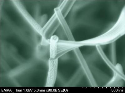
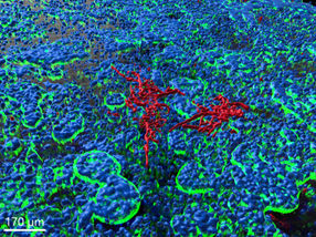
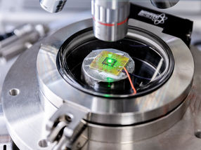
Under the scanning electron microscope (SEM), palladium octaethyl-porphyrin nano-lamellae and nanowires grow on a perylene nanowire which has been sputtered with silver particles.
Empa
The origin: an EU project called «PHODYE»
When Spanish physicist Angel Barranco returned to Valencia after a three year research stint at Empa, he initiated the EU project «PHODYE» with, among others, his old Empa colleagues. The aim is to develop highly sensitive gas sensors, for monitoring road vehicle emissions, for example, or for providing laboratory staff and mine workers with an early warning of the presence of poisonous substances. The sensors are based on fluorescing thin films which change color and fluoresce on contact with certain gas molecules.
"We were thinking in terms of a sort of electronic key for security applications, which would only react to certain optical conditions," explains Empa physicist Pierangelo Groening. Necessary for this are transparent, strongly fluorescing thin films, so Groening and Barranco developed a plasma-deposition process in order to store fluorescing dye molecules such as metallo-proyphins, perylenes and phthalocyanines unmodified and at high concentrations in SiO2 or TiO2 layers.
It soon became apparent that if certain gas molecules deposited on dye particles in the thin films, then these fluoresced at different wavelengths and the thin film changed color as a result. If different dyes are used then the gases which are toxic to humans can be detected at very low concentrations.
A surprisingly wide range of uses
However, for many sensor applications it is important that the response time be as short as possible, something which is hardly possible with compact plasma dye layers. It is, on the other hand, possible with layers which have very a porous structure, resembling the nap of a nanometer-scale carpet. Scientists hope to derive further benefits from such layers because they increase the area onto which the gas molecules to be detected can adsorb, and also shorten the diffusion distances, allowing the sensor to respond faster. Physicist Ana Borras thereupon developed a new vacuum deposition process for synthesizing organic nanowires.
In the meantime the Empa researchers made progress, learning how to manufacture nanowires with very widely varying characteristics by appropriately selecting the starting molecule and the experimental conditions. Nanowires of metallo-phthalocyanine molecules have diameters of a mere 10 to 50 nanometers and a length of up to 100 microns. What is unusual and unexpected about the new method is that by exactly controlling the substrate temperature, molecule flow and substrate treatment, the organic nanowires develop a previously unattained, perfectly monocrystalline structure.
Immediately after the first studies were made with the electron microscope it was clear to Groening that the new process could not only provide nanowires for the gas sensors but also make it possible to create complex "nanowire electric circuits" for electronic and optoelectronic applications such as solar cells, transistors and diodes. This is because the different types of nanowires can be combined as required to form networks with widely varying properties, as Groening and coworkers report in the scientific journal Advanced Materials and elsewhere.
The trick to achieving this lies in a second step in which the nanowires growing on the surface are "decorated" with silver nanoparticles by a sputter-coating process. A target, in this case a piece of solid silver, is bombarded with energetic ions, knocking off silver atoms which enter the gas phase and are deposited onto the nanowires. In a final step, the Empa team now grow more nanowires which, thanks to the silver particles, are in electrical contact with the original wires – the basis of an electrical circuit on the nanometer scale.
The first step from microelectronics to nanoelectronics
The first electrical conductivity measurements, made with the help of a four-tip scanning tunnel microscope in ultra high vacuum, exceeded the most optimistic expectations – the material is of an unusually high quality. "This opens up the possibility of soon being able to manufacture organic semiconductor materials," says Groening confidently. "And that, too, using a simple and economic process." In the meantime the researchers have successfully synthesized increasingly more complex structures of nanowires, and managed to link these together using a good deal of skill and a sure touch.
Take, for example, nanowires consisting of sections made with different starting molecules. If these molecules can transport either only positive or only negative charges, then a diode is created which allows current to flow in one direction alone. Groening speculates that it is quite possible that one day components for nanolectronics and nanophotonics will be made using this technique.
Original publication: A. Borras, O. Groening, J. Koeble, P. Groening; "Connecting Organic Nanowires"; Advanced Materials, vol. 21, issue 47, pp. 4816 - 4819
Other news from the department research and development


Get the analytics and lab tech industry in your inbox
From now on, don't miss a thing: Our newsletter for analytics and lab technology brings you up to date every Tuesday. The latest industry news, product highlights and innovations - compact and easy to understand in your inbox. Researched by us so you don't have to.