MIT: Tiny stamps for tiny sensors
New glass stamp may make cheaper, more precise biosensors
Advances in microchip technology may someday enable clinicians to perform tests for hundreds of diseases — sifting out specific molecules, such as early stage cancer cells — from just one drop of blood. But fabricating such “lab-on-a-chip” designs — tiny, integrated diagonistic sensor arrays on surfaces as small as a square centimeter — is a technically challenging, time-consuming and expensive feat.
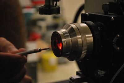
Now, researchers at MIT have come up with a simple, precise and reproducible technique that cuts the time and cost of fabricating such sensors. Nicholas Fang, associate professor of mechanical engineering, has developed an engraving technique that etches tiny, nano-sized patterns on metallic surfaces using a small, voltage-activated stamp made out of glass. Fang says the engravings, made of tiny dots smaller than one-hundredth the width of a human hair, act as optical antennae that can identify a single molecule by picking up on its specific wavelength.
“If you are able to create an optical antenna with precise dimensions … you can use them to report traffic on the molecular scale,” Fang says.
The researchers reported the new fabrication process in nanotechnology.
Hurdles to market
The new glass stamp approach may help researchers clear a large hurdle in lab-on-a-chip manufacturing: namely, scale-up. Today scientists fabricate nano-sensors using electron-beam lithography, an expensive and time-consuming technique that uses a focused beam of electrons to slowly etch patterns into metallic surfaces. The process, while extremely precise, is also extremely expensive: Fang says it’s common for facilities to rent such equipment out for $200 per hour. To fabricate a six-millimeters-squared pattern typically takes half a day — so if sensors made using electron-beam lithography were pushed into the commercial market, Fang estimates they would run more than $600 apiece.
“Nobody wants chips that expensive,” Fang says. “Biology tests are looking for something that’s cheap yet reliable. And that excludes some of the fancier, more expensive technologies.”
That may also exclude some cheaper technologies being developed today. For example, nanoimprint lithography is a simple, low-cost process where a moldable polymer is pressed onto a master circuit pattern. When exposed to UV light, the polymer hardens; when peeled off the master circuit, it forms a mold that can be filled with a metal substrate to make a copy of the original circuit pattern. Scientists typically wash the polymer mold away to isolate the new metallic pattern.
However, Fang says this approach, while inexpensive, can also be imprecise. The soft polymer material may not fit exactly around the original pattern, resulting in a mold with bumps, dents and other imperfections — and copies that aren’t exactly the same as the original. Since the process requires washing away the polymer mold, scientists need to use more polymer material to fabricate more copies.
A glass-blowing inspiration
Fang and his colleagues came up with a technique that may solve the cost, precision and reproducibility issues of other technologies. The team took an approach similar to nanoimprint lithography. But instead of polymer, the researchers used glass as a molding material.
“I was inspired by glassblowers, who actually use their skills to form bottles and beakers,” Fang says. “Even though we think of glass as fragile, at the molten stage, it is actually very malleable and soft, and can quickly and smoothly take the shape of a plaster mold. That’s at a large scale, but amazingly it works very well at a small scale too, at very high speed.”
With this in mind, Fang and his team cast around for a glassy material that would meet their requirements, and found an ideal candidate in a form of superionic glass — glass composed partly of ions, which can be electrochemically activated when pumped with voltage.
The researchers filled a small syringe with glass particles and heated the needle to melt the glass inside. They then pressed the molten glass onto a master pattern, forming a mold that hardened when cooled. The team then pressed the glass mold onto a flat silver substrate, and applied a small, 90-millivolt electric potential above the silver layer. The voltage stimulated ions in both surfaces, and triggered the glass mold to essentially etch into the metal substrate.
The group was able to produce patterns of tiny dots, 30 nanometers wide, in patterns of triangles, rectangles and, playfully, an ionic column, at a resolution more precise than nanoimprint lithography.
“You end up with a better cut,” Fang says. “And we have a stamp that can be reused many times.”
Fang acknowledges that there are still cost barriers to this glass-etching process: It still requires using a master metallic pattern, made via expensive lithography. However, he points out that only one master pattern, and one glass stamp, is needed to mass-produce an entire line of the same sensor, which may bring large-scale production closer to reality.
“With this stamp, I can reproduce maybe tens of hundreds of these sensors, and each of them will be almost identical,” Fang says. “So this is a fascinating advancement to us, and allows us to print more efficient antennae."
Other news from the department science


These products might interest you