Electrons zipping around in crystals
The end of the silicon age has begun. As computer chips approach the physical limits of miniaturization and power-hungry processors drive up energy costs, scientists are looking to a new crop of exotic materials that could foster a new generation of computing devices that promise to push performance to new heights while skimping on energy consumption.
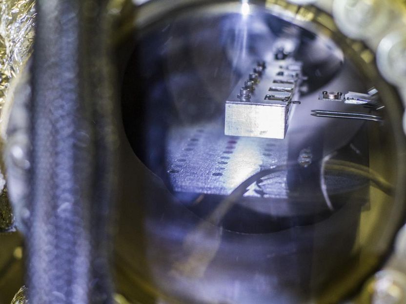
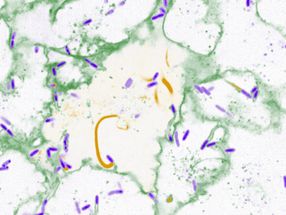
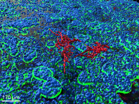
Extreme conditions are used to protect and preserve the TMDs during the experiments. As shown here, all samples are stored and manipulated in a vacuum that is close to the conditions in space.
Kyle Mittan/UANews
Unlike current silicon-based electronics, which shed most of the energy they consume as waste heat, the future is all about low-power computing. Known as spintronics, this technology relies on a quantum physical property of electrons -- up or down spin -- to process and store information, rather than moving them around with electricity as conventional computing does.
On the quest to making spintronic devices a reality, scientists at the University of Arizona are studying an exotic crop of materials known as transition metal dichalcogenides, or TMDs. TMDs have exciting properties lending themselves to new ways of processing and storing information and could provide the basis of future transistors and photovoltaics -- and potentially even offer an avenue toward quantum computing.
For example, current silicon-based solar cells convert realistically only about 25 percent of sunlight into electricity, so efficiency is an issue, says Calley Eads, a fifth-year doctoral student in the UA's Department of Chemistry and Biochemistry who studies some of the properties of these new materials. "There could be a huge improvement there to harvest energy, and these materials could potentially do this," she says.
There is a catch, however: Most TMDs show their magic only in the form of sheets that are very large, but only one to three atoms thin. Such atomic layers are challenging enough to manufacture on a laboratory scale, let alone in industrial mass production.
Many efforts are underway to design atomically thin materials for quantum communication, low-power electronics and solar cells, according to Oliver Monti, a professor in the department and Eads' adviser. Studying a TMD consisting of alternating layers of tin and sulfur, his research team recently discovered a possible shortcut.
"We show that for some of these properties, you don't need to go to the atomically thin sheets," he says. "You can go to the much more readily accessible crystalline form that's available off the shelf. Some of the properties are saved and survive."
Understanding Electron Movement
This, of course, could dramatically simplify device design.
"These materials are so unusual that we keep discovering more and more about them, and they are revealing some incredible features that we think we can use, but how do we know for sure?" Monti says. "One way to know is by understanding how electrons move around in these materials so we can develop new ways of manipulating them -- for example, with light instead of electrical current as conventional computers do."
To do this research, the team had to overcome a hurdle that never had been cleared before: figure out a way to "watch" individual electrons as they flow through the crystals.
"We built what is essentially a clock that can time moving electrons like a stopwatch," Monti says. "This allowed us to make the first direct observations of electrons move in crystals in real time. Until now, that had only been done indirectly, using theoretical models."
The work is an important step toward harnessing the unusual features that make TMDs intriguing candidates for future processing technology, because that requires a better understanding of how electrons behave and move around in them.
Monti's "stopwatch" makes it possible to track moving electrons at a resolution of a mere attosecond -- a billionth of a billionth of a second. Tracking electrons inside the crystals, the team made another discovery: The charge flow depends on direction, an observation that seems to fly in the face of physics.
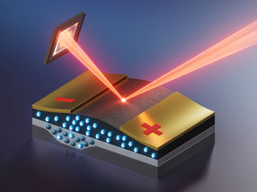
Collaborating with Mahesh Neupane, a computational physicist at Army Research Laboratories, and Dennis Nordlund, an X-ray spectroscopy expert at Stanford University's SLAC National Accelerator Laboratory, Monti's team used a tunable, high-intensity X-ray source to excite individual electrons in their test samples and elevate them to very high energy levels.
"When an electron is excited in that way, it's the equivalent of a car that is being pushed from going 10 miles per hour to thousands of miles per hour," Monti explains. "It wants to get rid of that enormous energy and fall back down to its original energy level. That process is extremely short, and when that happens, it gives off a specific signature that we can pick up with our instruments."
The researchers were able to do this in a way that allowed them to distinguish whether the excited electrons stayed within the same layer of the material, or spread into adjacent layers across the crystal.
"We saw that electrons excited in this way scattered within the same layer and did so extremely fast, on the order of a few hundred attoseconds," Monti says.
In contrast, electrons that did cross into adjacent layers took more than 10 times longer to return to their ground energy state. The difference allowed the researchers to distinguish between the two populations.
"I was very excited to find that directional mechanism of charge distribution occurring within a layer, as opposed to across layers," says Eads, the paper's lead author. "That had never been observed before."
Closer to Mass Manufacturing
The X-ray "clock" used to track electrons is not part of the envisioned applications but a means to study the behavior of electrons inside them, Monti explains, a necessary first step in getting closer toward technology with the desired properties that could be mass-manufactured.
"One example of the unusual behavior we see in these materials is that an electron going to the right is not the same as an electron going to the left," he says. "That shouldn't happen -- according to physics of standard materials, going to the left or the right is the exact same thing. However, for these materials that is not true."
This directionality is an example of what makes TMDs intriguing to scientists, because it could be used to encode information.
"Moving to the right could be encoded as 'one' and going to the left as 'zero,'" Monti says. "So if I can generate electrons that neatly go to the right, I've written a bunch of ones, and if I can generate electrons that neatly go to the left, I have generated a bunch of zeroes."
Instead of applying electrical current, engineers could manipulate electrons in this way using light such as a laser, to optically write, read and process information. And perhaps someday it may even become possible to optically entangle information, clearing the way to quantum computing.
"Every year, more and more discoveries are occurring in these materials," Eads says. "They are exploding in terms of what kinds of electronic properties you can observe in them. There is a whole spectrum of ways in which they can function, from superconducting, semiconducting to insulating, and possibly more."
The research described here is just one way of probing the unexpected, exciting properties of layered TMD crystals, according to Monti.
"If you did this experiment in silicon, you wouldn't see any of this," he says. "Silicon will always behave like a three-dimensional crystal, no matter what you do. It's all about the layering."
Original publication
Other news from the department science


Get the analytics and lab tech industry in your inbox
From now on, don't miss a thing: Our newsletter for analytics and lab technology brings you up to date every Tuesday. The latest industry news, product highlights and innovations - compact and easy to understand in your inbox. Researched by us so you don't have to.
Most read news


More news from our other portals


See the theme worlds for related content
Topic World Spectroscopy
Investigation with spectroscopy gives us unique insights into the composition and structure of materials. From UV-Vis spectroscopy to infrared and Raman spectroscopy to fluorescence and atomic absorption spectroscopy, spectroscopy offers us a wide range of analytical techniques to precisely characterize substances. Immerse yourself in the fascinating world of spectroscopy!